As anyone who has ever assembled a run of PCBs will tell you, quality inspection of solder joints can be a difficult process. Even under a microscope their appearances can be deceptive, and one silver blob can be perfect while its neighbour conceals a problem. The electronics industry have developed inspection tools to help, including optical inspection devices. It’s one of these that [Sina Roughani] has built, in the form of a hemispherical 3D printed dome with concentric rings of coloured LEDs mounted within it.
The principle behind this tool is as unexpected and simple as it is clever; by having different colours of light from different elevations of the dome it ensures that each different angle of the solder joint surface reflects a different colour. Thus a colour photograph shot from directly above the board allows visual inspection of the quality of the solder joints by the rainbow of colours that appears around their edges. This process can even be automated with OpenCV or similar, hence the process is referred to as Automated Optical Inspection, or AOI.
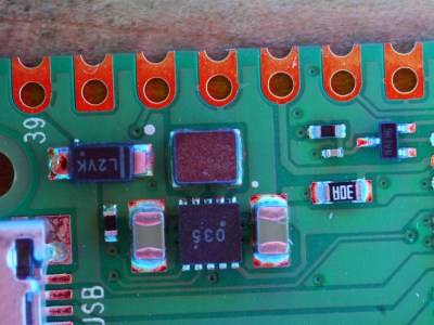
The technique is demonstrated with some pictures of a Raspberry Pi Pico, on which it shows really well the rainbow-edged solder joints and the red colour reflected from flat pads. What at first might seem like a novelty lighting effect becomes a very useful inspection tool.
PCB inspection is a subject we’ve covered before, though perhaps we don’t all have access to X-rays.
Source:: Hackaday