Electron microscopes were once the turf of research laboratories that could foot the hefty bill of procuring and maintaining such equipment. But old models have been finding their way into the hands of eager individuals who are giving us an inside look at the rare equipment. Before you start scouring Craigslist, go on a crash course of what you need to know with Adam McComb’s Hacker’s Guide to Electron Microscopy. He presented the talk at the 2018 Hackaday Superconference and the recording was just published, you’ll find it below.
Two Ways to Make the Really Small, Big
The first thing you need to know about these instruments is that there are two categories: Transmission Electron Microscopes (TEM) and Scanning Electron Microscopes (SEM).
Though it might seem tempting, you probably don’t want to get involved with a TEM. These microscopes operate by shining electrons through a sample onto a phosphor target; the phosphors glow, building the image. With a TEM you can achieve incredible resolution — on the atomic scale — and do things like taking pictures of viruses and even reconstructing neural connections in the brain. But all this comes at the cost of higher complexity. Samples need to be very thin, on the order of 70-100 nanometers, which means you would need access to specialized cutting tools such as diamond knives and ion beam milling. The optical path is incredibly complex, and chemicals to prepare samples can be quite hazardous.
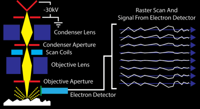
On the other hand, Scanning Electron Microscopes (SEM) are well within reach of the home workshop. They function by aiming an electron probe at a sample and counting the number of electrons that bounce back at each discrete location to judge brightness. These are the instruments that hackers are starting to have in their garages and workshops.
SEM Capabilities and Workflow
In his talk, Adam illustrates some of the extended features of an SEM in examining integrated circuits — you can use one to do much more than simply making pictures. The primary electron beam generates those secondary electrons bouncing back to the sensor to form an image of the surface of the sample. But at higher voltages, backscatter electrons will also be generated which can be used to derive its chemical makeup. With the proper sensing equipment, characteristic X-Rays generated when an excited ion in the sample falls back to its ground state can be used to determine the sample material. Combining these means looking beneath the surface of the die to judge what materials are present and where they go. Effectively you are now reverse engineering the layers in an IC design.
Adam dips into details of the sample prep process, which is much easier than with a TEM but which still requires a bit of effort. Samples need to be electrically conductive so that electrons bounce off instead of being absorbed, and this usually involves sputter in an argon and gold process. Since they will be observed in a …read more
Source:: Hackaday