The software takes one layer of the PCB layout, converts it to black and white, and then runs a C++
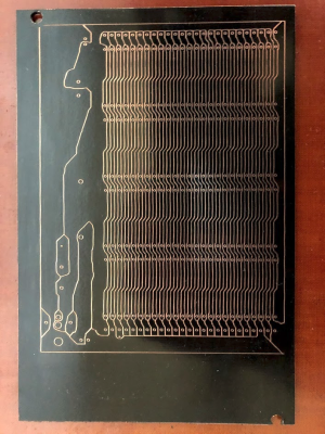
Tuning a desktop router and your board designs for isolation routing can be a bit tricky, with thin traces usually being the first victim. For simple prototype boards you usually don’t need tightly packed traces, you just want to isolate the nets. To do this with a minimum amount of routing, [Michael Schembri] created kicad-laser-min, a command-line utility that takes a Kicad PCB design and expands all the tracks and pads to their maximum possible width.
The software takes one layer of the PCB layout, converts it to black and white, and then runs a C++ Voronoi algorithm on it to dilate each track and pad until it meets another expanding region. Each region is colourised, and OpenCV edge detection is used to produce the contours that need to be milled or etched. A contour following algorithm is then used to create the G-code. The header image shows the output of each step.
Full source code is available on GitHub. [Michael] has had good results with his own boards, which are scribed using a laser cutter before etching, but welcomes testing and feedback from other users. He has found that OpenCV doesn’t always completely close all the contours, but the gaps are usually smaller than the engraving width of his laser, so no shorts are created.
This is basically “Scribble style” prototyping with CAD and CNC tools. If you prefer scribe and etch, you might consider building a simple PCB shaker for faster etching. If you have a router but want to avoid the dust, you can use a carbide scribe to scratch out the tracks without needing to etch.
Source:: Hackaday