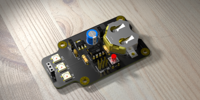
We seem to want our PCB design software to do everything these days, and it almost delivers. You can not only lay it all out, check electrical and design rules, and even spit out a bill of materials, but many PCB tools produce 3D models that are good enough to check parts clearance or are useful in designing enclosures. But when it comes to producing photorealistic output, whether for advertising or just for eye-candy, you might want to turn to 3D design tools.
In this workshop, Anool Mahidharia takes the output of KiCad’s VRML export, gets it rendering in Blender, and then starts tweaking the result until you’re almost not sure if it’s the real thing or a 3D model. He starts off with a board in KiCad, included in the project’s GitHub repo, and you can follow along through the basic import, or go all the way to copying the graphics off the top of an ATtiny85 and making sure that the insides of the through-plated holes match the tops.
If you don’t know Blender, maybe you don’t know how comprehensive a 3D modelling and animation tool it is. And with the incredible power comes a notoriously steep learning curve up a high mountain. Anool doesn’t even try to turn you into a Blender expert, but focuses on the tweaks and tricks that you’ll need to make good looking PCB renders. You’ll find general purpose Blender tutorials everywhere on the net, but if you want something PCB-specific, you’ve come to the right place.
Anool is an electrical engineer by day and a Hackaday contributor by night. He has written a bunch of articles on KiCad, including this classic on managing component libraries that we still refer to, and this introduction to the cool things you can do with action plugins. He also practices what he preaches, and has designed a number of cool open-source hardware projects and even the badge for the Open-Source Hardware Summit.
Source:: Hackaday

